Basic Voltage-Controlled Amplifier

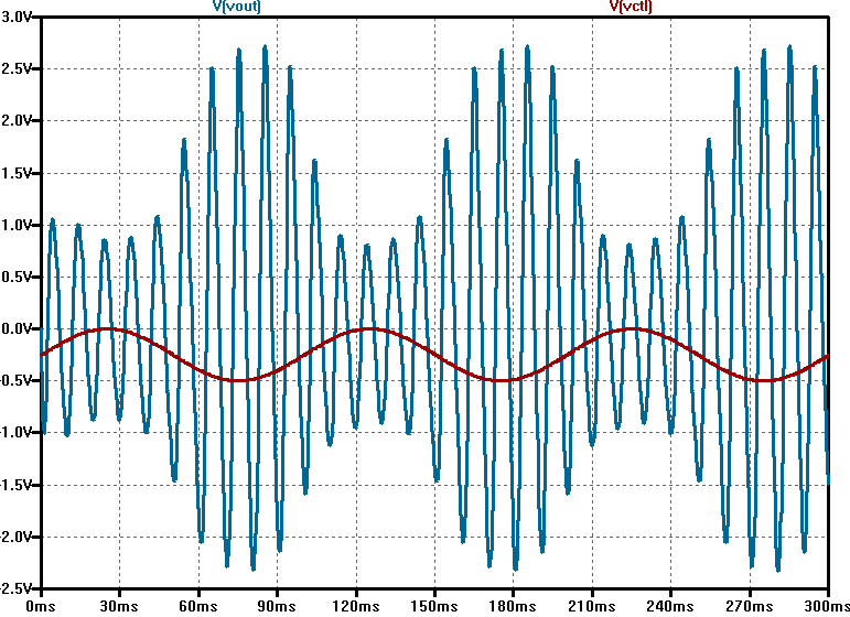
I’ve been looking at the theoretical principles that govern the voltage-controlled amplifier (VCA) recently and came across some simple VCA designs that caught my attention. A common technique involves a JFET and an opamp to achieve VCA type operation by using the JFET as a voltage-controlled resistor somewhere in the input path. I’ve seen a good deal of these circuits out there, but I had trouble getting good simulation results from what I had seen. I cam across an article by Rod Elliot of Elliot Sound Products which covered some nice history and interesting discussion of the VCA in general. After going over the information there, I came up with this design based on some of the more basic designs presented.

Basic VCA LTSpice Schematic

One of the things I’ve been most interested in is trying to accomplish this with a single supply which is common in most stompbox setups. In the schematic, there’s an emitter-follower stage just to act as a buffer for the input signal followed by an inverting opamp stage. To make this work, both C1 and C2 are required to effectively AC couple both input signals (Vin and Vctl) to the opamp stage. There’s an RC network that is supposed to tame the distortion in the output by taking a portion of the output and connecting it to the input of the J201. The article explains this in decent detail. In simulation, the it seems to smooth out the non-linearity of the JFET as Vctl changes. Using the J201, LTSpice gives a decent linear-like response over a range of around 500 mV (0 to -500 mV at the input) and operates decently with a 500 mVp signal.

VCA Linearity Test

For use with an LFO, I found that the best results happen with a slight negative voltage offset and a signal who’s amplitude peaks at 0V (i.e. 250 mV sinusoidal signal with a -250 mV offset). Of course, this is all highly dependent on the threshold voltage of the J201 which can range from -0.3 V to -1.5 V according to the Fairchild datasheet. It will be interesting to see the results of this circuit on a breadboard.

LFO modulated VCA Simulation

References:
[1] Gray, P. (2009). Analysis and design of analog integrated circuits. New York: Wiley.

[2] Sound.whsites.net. (2017). VCAs. [online] Available at: http://sound.whsites.net/articles/vca-techniques.html [Accessed 1 Sep. 2017].

MOSFET vs. BJT

a good rule of thumb pulled from this forum thread (http://www.electro-tech-online.com/general-electronics-chat/39339-mosfet-vs-bjt.html):

  1. Need a switch to be fully-on fully-off and carry lots of current -MOSFET
  2. Need a switch that needs to have lowish capacitance – BIPOLAR
  3. Need a cheap, dirty 2 or 3 component current source – BIPOLAR
  4. Need a low voltage/noise amplifier – BIPOLAR
  5. Need an amplifier with VERY low input/bias current – MOSFET
  6. Need a low noise AND low input current amplifier – JFET
  7. Need a one component current source – JFET
  8. Need switch or amp that must cost almost nothing – BIPOLAR
  9. Need multiple transistor package that has matching – BIPOLOAR
  10. Need switch that may be over-voltaged – MOSFET
  11. need switch/amp that sits in nasty RF environment – MOSFET (BIPOLARS rectify & cause offsets)


MOSFETs can generally switch faster (they certainly require less complex and less power to drive their gates). But if I’m not mistaken, BJTs designed for the task can switch very very fast since they have no gate capacitance to charge and can also operate in quasi-saturation mode for even faster switching at the expense of conduction efficiency. MOSFETs have less losses when used as a switch at “lower” voltages (lower as in industry’s definition which is <~200V). MOSFETs act like a resistor when on while BJTs act more like diodes. The resistance can be modified by changing the “dimensions” of the MOSFET while the BJT’s “diode voltage drop” can’t be changed so easily unless the materials are changed. THis tends to make MOSFETs have less losses at the lower voltages but also means MOSFETs can be paralleled since current imbalances will cancel out. With parallel BJTs, the best BJT will hog the current from the other “not so good BJTs” and burn out and the cycle repeats with the remaining BJTs until they are all burned. This is similar to parallel diodes. You can correct for imbalances by manually tuning resistors in series with each BJT, but for power applications that’s needing massive resistors and wasting lots of power.

thanks guys…