Basic Voltage-Controlled Amplifier

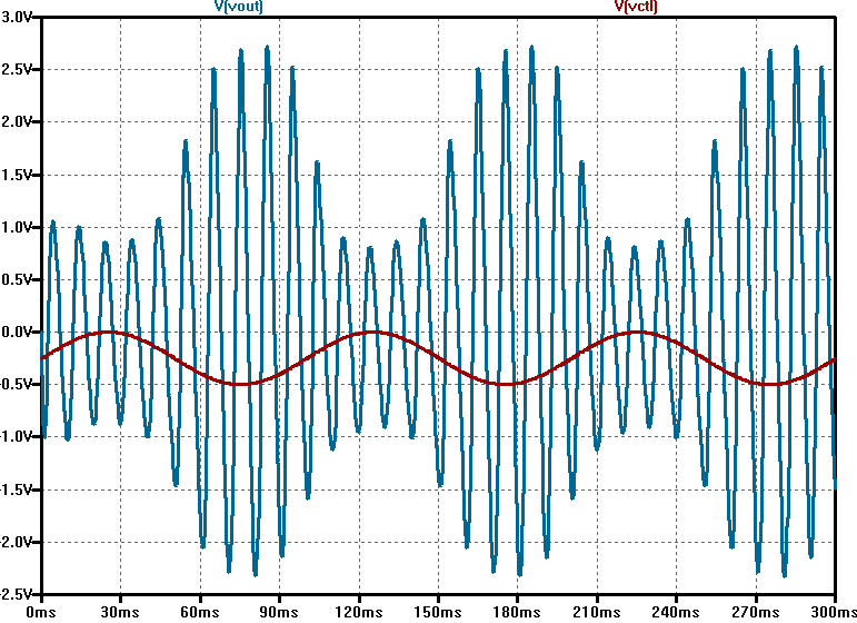
I’ve been looking at the theoretical principles that govern the voltage-controlled amplifier (VCA) recently and came across some simple VCA designs that caught my attention. A common technique involves a JFET and an opamp to achieve VCA type operation by using the JFET as a voltage-controlled resistor somewhere in the input path. I’ve seen a good deal of these circuits out there, but I had trouble getting good simulation results from what I had seen. I cam across an article by Rod Elliot of Elliot Sound Products which covered some nice history and interesting discussion of the VCA in general. After going over the information there, I came up with this design based on some of the more basic designs presented.

Basic VCA LTSpice Schematic

One of the things I’ve been most interested in is trying to accomplish this with a single supply which is common in most stompbox setups. In the schematic, there’s an emitter-follower stage just to act as a buffer for the input signal followed by an inverting opamp stage. To make this work, both C1 and C2 are required to effectively AC couple both input signals (Vin and Vctl) to the opamp stage. There’s an RC network that is supposed to tame the distortion in the output by taking a portion of the output and connecting it to the input of the J201. The article explains this in decent detail. In simulation, the it seems to smooth out the non-linearity of the JFET as Vctl changes. Using the J201, LTSpice gives a decent linear-like response over a range of around 500 mV (0 to -500 mV at the input) and operates decently with a 500 mVp signal.

VCA Linearity Test

For use with an LFO, I found that the best results happen with a slight negative voltage offset and a signal who’s amplitude peaks at 0V (i.e. 250 mV sinusoidal signal with a -250 mV offset). Of course, this is all highly dependent on the threshold voltage of the J201 which can range from -0.3 V to -1.5 V according to the Fairchild datasheet. It will be interesting to see the results of this circuit on a breadboard.

LFO modulated VCA Simulation

References:
[1] Gray, P. (2009). Analysis and design of analog integrated circuits. New York: Wiley.

[2] Sound.whsites.net. (2017). VCAs. [online] Available at: http://sound.whsites.net/articles/vca-techniques.html [Accessed 1 Sep. 2017].

DOD FX55B SupraDistortion – BigBuff Mod

wpid-20140915_140854.jpg

Here’s another in a line now of DOD pedal mods. For this FX55B, I decided to go for more of a BigMuff sound. Playing around with this pedal initially, I found it to be like most mass-produced distortion/fuzz effects. It had a very thin sound and that notorious volume drop that you may have heard on a high-school band’s first album. The lows were almost non-existent when the effect was engaged. I found the following schematic and, with a few simple changes, came out with a distortion pedal with considerable gain, massive lows, and a smoother, more rounded square wave.

dodfx55b_bigbuff_mod

Overall, the idea here was to get more from the pedal by employing some germanium to smooth out the harshness and to increase the overall output. The output is now considerably higher as long as the tone knob is set closer to 10 o’clock. At noon, the mixing is practically useless. At the 4 o’clock position, you get more of a thin, trash punk type of sound with an excessive noise floor. The sound sample demonstrates the effect with the tone set at about 10:30-11 and first contrasts the distortion setting. The third set shows off the tone below 10 o’clock. The last set shows what the tone does when you sweep through it.

TDA2040-based amp schematic with EQ…

well here’s the first draft of the simplest medium powered solid state design i could muster. TL082 can easily be substituted with a TL072 which is probably better anyhow (i just have all these TL082s laying around). the power supply i’m using more like 14-15V. both ICs should easily be able to handle up to 20V and that would allow for louder operation, but i think 15V is safe. all the resistors are 1/8W minus R20 which is 1/4W.

Bending notes with PT2399…

i’ve been experimenting with this PT2399 chip and using various schematics to create a digital delay circuit. the delay time seems to be directly attached to the sample rate since lengthening the delay time gives a nice decrease in pitch. i’m toying with the idea of dropping a time constant in around the controlling delay time circuit to see about achieving a “tape warble” sort of effect. we’ll see what works.

here’s the schematic i’ve been working with though the values i’m using are hardly similar.

[audio:http://abrammorphew.com/notes/wp-content/uploads/2010/11/pt2399-demo01.mp3|titles=pt2399-demo01]